Increasing demand of key semiconductor performance parameters is not being met by traditional materials
Typical wide bandgap (WBG) materials such as silicon carbide (SiC) and gallium nitride (GaN) are reaching their theoretical limits for high-power and high-temperature applications. They cannot meet the increasing demand of key performance parameters such as high reverse breakdown voltage, high switching speed, and low forward conduction loss. While aluminum nitride (AIN) offers superior energy bandgap, saturation velocity, critical electrical field, thermal conductivity, and Johnson’s figure of merit (JFOM), it suffers from inefficient doping and very few carriers of electricity, electrons, or holes due to a reconfigurable defect formation that causes an increase in dopant activation energy.
Metal modulated epitaxy method uses crystal synthesis to impede dopant reconfiguration and enable superior AlN semiconductors
The metal modulated epitaxy (MME) method enables the production and use of p-type beryllium-doped AlN (AlN:Be) films as key components in ultra-wide bandgap (UWBG) semiconductors for the first time. These films can be used in high-power and high-temperature diodes and transistors. The unique MME method is performed with widely available, commercial molecular beam epitaxy reactors to grow the films, overcomes safety concerns of beryllium-doping using traditional metalorganic chemical vapor deposition (MOCVD) methods, and enables substantial p-type conduction not observed prior to this work. The method improves current conduction over best previous results in p-type AlN by 30,000,000 times and n-type AlN by 6,000 times.
Using crystal synthesis methods that generate fewer compensating impurities and less lattice expansion impedes the reconfiguration of dopants and results in well-behaved bulk semiconducting functionality in AlN, creating the largest direct bandgap semiconductor known. It produces a substantial bulk p-type conduction, a dramatic improvement in n-type bulk conduction, and a P-N junction AlN diode with a nearly ideal turn-on voltage.
There are four extensions of the MME method, which can be used:
- To create materials for junction barrier Schottky (JBS) diodes
- To create materials for Schottky barrier diodes (SBDs)
- With GaN to make layered films to improve current uniformity
- With a nickel mask to add structural mesas to GaN films to improve switching speeds
JBS diodes and SBD
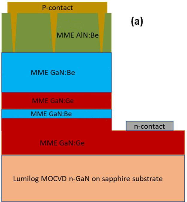
JBS diodes are advanced structures that achieve high breakdown voltage with good forward voltage characteristics. Using MME results in a simpler fabrication method to construct a JBS diode with a higher breakdown performance. This new form of JBS diode is created by exploiting the cracking that results from lattice mismatch between AlN and GaN. This JBS diode incorporates a p-type AlN layer grown beyond the crack formation thickness on top of the unintentionally doped (UID) layer. Because the cracks extend down to the UID layer, Schottky metals deposited on the surface will cover the p-type AlN and contact the UID layer, forming cyclic Schottky diodes in the crack gaps separated by p-AlN/UID/n-type GaN diodes adjacent to the Schottky diodes.
A high breakdown, high-power SBD can be created using the MME method to grow AlN:Be in layers along with additional levels of doping of AIN. This new Schottky diode utilizes Be-doped AIN to create UWBG semiconductors for high-power, high-frequency devices capable of operation in extreme heat and radiation environments.
Thin current spreading layers
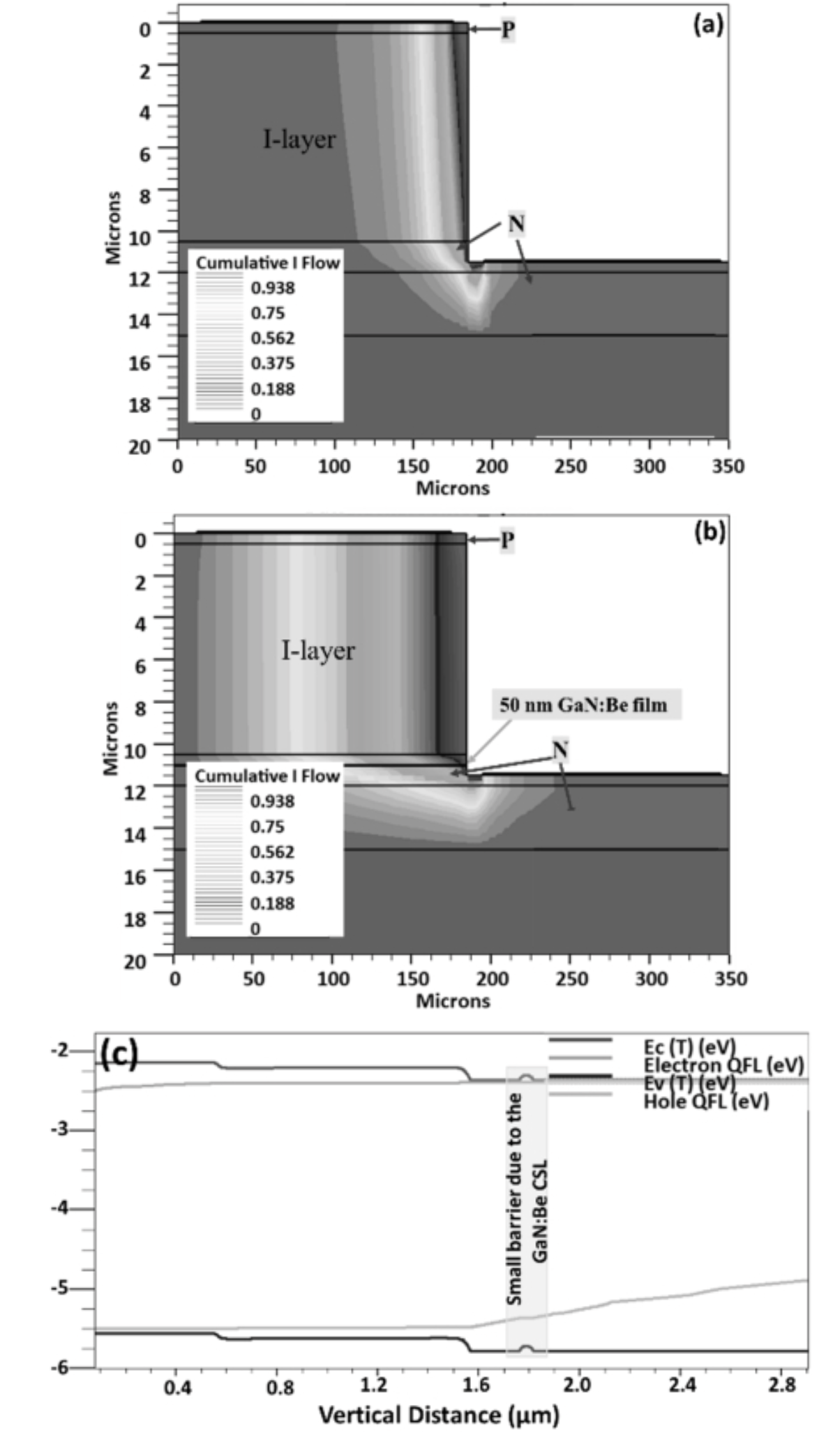
The MME method has been used to demonstrate a new approach to current spreading in quasi-vertical diodes that avoids excessive current flow, field crowding, and premature breakdown at the mesa edges. It does this by improving electrical current uniformity in group III-nitride devices with thin current spreading layers (CSLs). By sandwiching a thin gallium nitride (GaN):beryllium (Be) intrinsic layer (i-layer) thin film inside the n-type GaN layer, the current uniformity dramatically increases from approximately 40% of the p-contact radii to nearly 100%, resulting in higher breakdown performance and reduced current leakage. This technology can be applied to any thickness drift layer and has been shown to be particularly effective for thicker drift layers needed for high-voltage devices. It can be used for any Ga-containing alloy (e.g., aluminum-gallium-indium-nitride [AlGaInN]).
While demonstrated with Georgia Tech’s MME method, the high breakdown voltage and good forward voltage characteristics of these devices may enable comparatively high performance in group III-nitride high-power devices even when grown by other methods.
Cascaded nickel hard mask
The MME method can also create thick layers for protecting semiconductor regions of power devices during fabrication to prevent damage that often occurs during the plasma etching process. This new approach can be used to create the deep vertical mesas necessary for many high-power devices, while addressing damage caused by plasma etching by utilizing a combination of a cascaded e-beam deposition and sputtering of nickel to form a cascaded nickel hard mask. This method has successfully achieved GaN mesas up to 13 microns in MME-grown pin devices.
The robust nickel hard mask can withstand plasma etching for the length of time necessary to protect the semiconductor regions underneath the mask without adhesion issues found in other thick metal mask approaches, and without forming chemical alloys that damage the semiconductor intended to be protected. The combination of the hard mask technology and lithography is a scalable method that has the potential to increase the speed and consistency of production of commercial high-power electronic and optoelectronic devices.
With the ability to handle over five times the voltage of existing WBG semiconductors, AlN enables applications that will impact high-temperature, high-voltage, and high-power electronics; deep ultraviolet light-based viral and bacterial sterilization; polymer curing; lithography; laser machining; and more.
- Enables high-quality semiconductors: Leverages MME method to provide the first access to p-type AlN:Be films, a superior UWBG semiconductor material to create high-power, high-temperature diodes and transistors.
- Ease of fabrication: Avoids costly and complicated methods unfavorable for beryllium doping.
- Improved breakdown performance: Achieves high reverse breakdown voltage—a significant advantage over WBG materials such as SiC and GaN.
- Higher efficiency: Leverages the critical electric field of doped AIN, which is three times that of GaN, five times SiC, and 50 times silicon (Si).
- Increased current conduction: The method improves current conduction over best previous results in p-type AlN by 30,000,000 times and n-type AlN by 6,000 times.
- Customizable: Accommodates various dopants (Be, C, or p-type) and flexible selection of anode and cathode metals, thereby enabling control of the forward conduction and reverse breakdown voltage for a range of high-power AlN Schottky diode applications.
- Substantially deeper etches: Because a very thick metal mask can be created, a wide range of µm features can be etched in a variety of group III-nitride semiconductors, allowing for extremely high-voltage devices that require thicker layer structures.
- Robust: This method has demonstrated highly consistent and effective protection against the kind of damage that is typical with standard fabrication methods.
- Scalable: The nickel hard mask with cascaded e-beam evaporation and sputtering metal deposition method can readily be applied to the large-scale production of electronic devices.
- Cost-effective: By reducing the breakage and damage that is common in the production of high-power electronic devices, this method has the potential to greatly reduce the high costs of lost labor and wasted materials.
- Increases current uniformity: Improves cumulative current flow distribution from ~40% to ~100% of the p-type contact.
- High performance: Avoids premature breakdown at the mesa edges making quasi-vertical devices comparable in performance to more expensive vertical devices.
- Improves immunity to etch variation: Because current flow is no longer crowded along the mesa edges, process-related variations in the mesa etching are less important to the diode performance.
- UWBG semiconductors for high-power, high-voltage, high-frequency devices capable of operation in extreme heat and radiation environments
- Group III-nitride devices for electronic and optoelectronic applications (e.g., rectifying diodes for power, radio frequency and communications, solar cells, light-emitting diodes, photodetectors, and laser diodes)
- GaN-based deep ultraviolet, high-power, and high-frequency devices

Layer structure diagram of quasi-vertical AIN JBS diode that uses intentionally cracked layers to form periodic JBS structures.

These figures show a pin diode structure having: (a) 10 μm UID GaN i-layer and (b) 10 μm GaN:Be i-layer and 50 nm GaN:Be thin film sandwiched in the n-type GaN layer. Current uniformity is improved from ~40% in (a) to ~100% in (b). Figure (c) is an energy band diagram of (b) for a 1 μm i-layer under forward bias indicating a small energy barrier introduced by the thin GaN:Be current spreading layer.
