There is a need for reusable radiation monitors that don’t require constant power
Current radiation detectors are either single-use, film-based badges that must be developed using a chemical process similar to photographic film, or they are electronic devices that require constant electric power to operate. Both have disadvantages and limitations. For example, developing the single-use, film-based badges take time and reading the results can be somewhat subjective. The electronic devices are limited to applications in which electric power is constantly available.
Ionizing radiation detection device enables micropower monitoring
This innovative radiation detection system provides real-time, on-demand detection in a versatile, micropowered design. It detects both ionizing radiation and neutron radiation using configurations of materials varying from one-atom thick to multiple-atom thicknesses (e.g., graphene or graphene nanoribbons) to quasi-two-dimensional materials or thin films (e.g., hexagonal boron nitride) to topological materials (e.g., bismuth selenide and tungsten diselenide).
The system’s micropower operation is due to its exposure to radiation, which results in changes to the device’s electrical properties, even in the absence of voltages and currents. These changes occur because electrical resistance parallel to the plane of the conductive layers is affected by the passage of ionizing radiation or neutrons (which may undergo a neutron-capture reaction during passage). Radiation exposure is calculated and readable on demand as a function of that resistance.
The versatility of this design, which can employ polymeric encapsulation, can result in mechanically flexible detectors with on-demand electronic read-out of cumulative radiation doses and micropower operation. It can be used for large-area or single-particle detectors.
- Micropower operation: The device materials offer higher conductivity (mobility) than silicon, resulting in reduced power needs (i.e., requiring power only during read-out).
- Reusable and on-demand: Readout of the integrated dose of radiation received by the device is available on demand at any time, creating a reusable device for continuous radiation detection.
- Versatile: Independent selection and layering of channel and gate materials enables tuning devices for different radiation types, including options for polymeric encapsulation that offer potential to create flexible radiation-sensitive “patches.”
- Ultrafast dynamic response: Real-time monitoring of dynamic changes (microsecond to nanosecond time scales) can detect single-particle events.
- Expandable: The broad range of possible 2D and topological materials creates potential for other types of detection.
Detection of neutrons and ionizing radiation in:
- Space
- Spacecraft or spacesuit monitoring (e.g., lunar and other deep space missions where organ-specific radiation monitoring of humans and animals will be necessary)
- Off-planet agriculture monitoring
- Medical facilities
- Nuclear reactors
- Nuclear weapons facilities
- Terrorism prevention (e.g., monitoring of potential nuclear material)
- Soldiers and other at-risk personnel
![(Left) Device concept showing current (I), voltage (V), and gate voltage (Vg). (Right) Early device prototype. (Further development focuses on developing methods for additive manufacture of the devices [e.g., inkjet printing].) 4 electrical contacts with an orange rectangle between them atop a 3-layer base (Vg). Connectors run between center 2 (V) and outer 2 (I). Photo with orange background and 4 horizontal gold lines overlaid with a black square on a white square and extending wires.](/sites/default/files/2023-06/Sensor2.png)
(Left) Device concept showing current (I), voltage (V), and gate voltage (Vg).
(Right) Early device prototype. (Further development focuses on developing methods for additive manufacture of the devices [e.g., inkjet printing].)

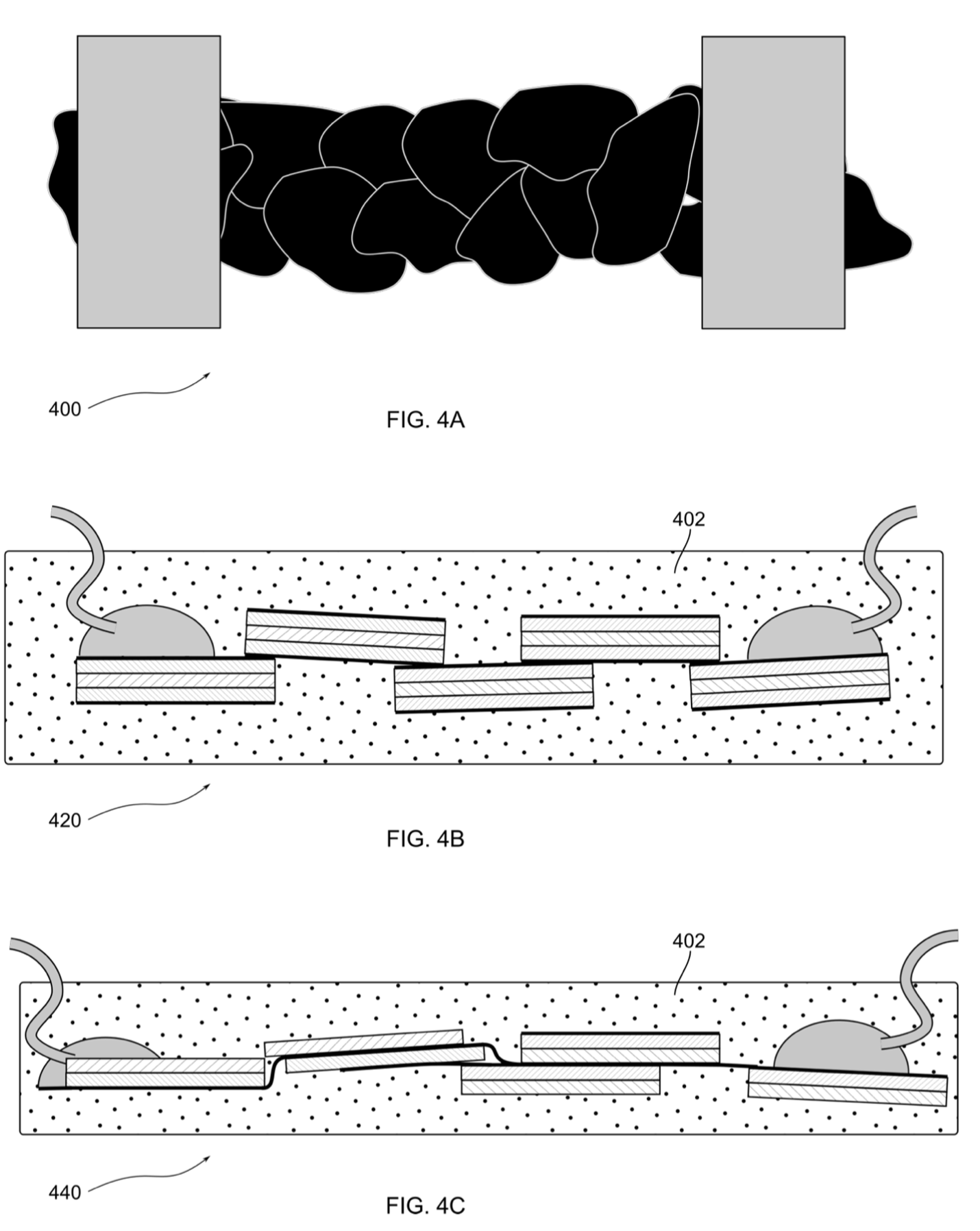
Figure 4A shows the layering ordered within flakes of materials but discontinuous between flakes. The proximity of flakes is such that electrical continuity is maintained from one electrical contact to the other (and to more electrical contacts, if required by the style of resistance measurement). In Figure 4B, a cross-sectional view shows encapsulation in a protective insulating material 402. Figure 4C illustrates that within any of the embodiments incorporating flakes of materials, the layer stacking need not be perfectly ordered, even within a single flake.
