Cost of existing nanoscale printing technology prohibits widespread use and scalability
Nanoscale patterned metallic thin films are vital components in nano-enabled devices and applications such as electrical interconnects in high-density printed electronics, plasmonics-based meta-materials for bio-sensing and optical modulation, and microelectromechanical systems. Current femtosecond laser-based techniques used to print complex 2D and 3D structures are slow and expensive, and often unaffordable for low and moderate-volume manufacturing applications.
High-intensity femtosecond lasers can overcome optical diffraction limits, but are costly. The current technology is also limited by a slow, sequential printing mechanism. An alternative light-based printing system is needed that eliminates expensive lasers while also achieving precise, detailed nanoscale printing of polymers and metals.
Low-intensity, low-cost superluminescent light system improves nanoscale printing accessibility
This SLP system offers several advantages for the process of nanoscale printing: lower cost, higher speed, and finer resolution. The light source is a superluminescent light emitting diode (SLED) that is 100 times less expensive than the lasers in current use, leading to an overall decrease in printing costs of 10–50 times. Utilizing the specific effects of superluminscent light projection, sharp-edged images with minimal speckling patterns are created, resulting in high-resolution images and structures on both polymer and metal-based films.
And, by implementing a parallel writing mechanism, this system generates significant improvements in throughput speed— up to 100 times faster than existing metal printing methods and four times faster than existing polymer printing methods. These benefits create a readily scalable system for a variety of industrial needs and make nanoscale printing a viable resource for a larger manufacturing audience.
- Less Expensive: This system uses an inexpensive, readily available SLED that is 100 times less costly than the femtosecond lasers used with current technology (overall, decreasing nanoscale printing costs by 10–50 times).
- Faster: The SLP system uses a parallel writing system, allowing higher throughput speeds—at least 100 times faster for metal printing and four times faster for polymer printing.
- Flexible: Unlike other nanoscale printing technologies, this system enables both polymer and metal printing.
- Scalable: Lower lighting costs, higher printing speeds, and the potential for stacking of 2D layers to create 3D structures make this system useful in a wide range of manufacturing situations.
- Higher resolution: Using a high-numerical-aperture oil-immersion lens with superluminescent light allows greater capture of oblique light, resulting in finer resolution printing.
- Micro-optics for quantum devices
- Metaphotonics for flat optics and photonic quantum devices
- Printed structures for light directing chips (LIDAR in self-driving cars)
- Microfluidics chips and microrobots for biomedical and drug delivery applications
- Printed electronics
- Printed batteries

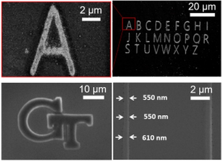
Exemplary nanoscale structures printed with the SLP system. Metal structures are shown on the top row and polymer structures are shown on the bottom row.
