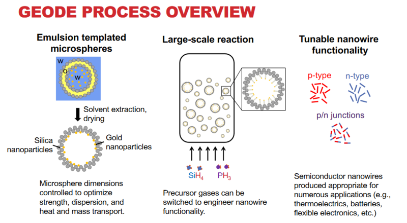
Inventors at Georgia Tech have developed a novel process that can overcome the challenges of nanowire fabrication that is flexible, rapid and user programmable. Initially, hollow microspheres are synthesized in bulk quantities via an emulsion templating technique. The walls of these porous microspheres enable facile mass/heat transport while the metal nanoparticles, which decorate the interior, serve as catalysts for nanowire growth. While the microspheres are fluidized in a continuous flow CVD reactor, nanowire voxels grow on the microsphere interior surface. Each voxel is designed with lock-and-key tips and functional blocks that impart the desired properties to the final product. Through the use of entropic depletion interactions that induce a preferential attraction between bodies with complementary shapes (i.e. lock-and-key), the nanowire voxel building blocks are harvested and assembled into larger superstructures.
- Greater than 106 improvement in the rate of nanowire synthesis compared with the current state-of-the-art
- Applicable to diverse classes of materials, dopant concentrations, and morphologies
- Superstructure assembly is programmable via tip geometry and is material independent
- Able to fabricate nanowire voxels into n-and p-type doped superstructures with thermal conductivities below 1 W m-1K-1
This invention will enable the scalable production of functional nanowire voxel building blocks for a broad range of advanced electronic materials. The realization of a high throughput fabrication process will enable innovations in electronic component cooling, transportation, and military applications. These materials also have the potential to revolutionize power generation by converting waste heat into electricity without producing greenhouse emissions.
Semiconductor nanowires are promising building blocks for innumerable advanced materials and devices, such as thermoelectrics, light emitting diodes, solar cells, and cellular scaffolds. Despite their potential, a need remains for an efficient and large-scale process for the fabrication of semiconductor nanowires with the dimensions, dopant concentrations, and spatial arrangements that are required of real-world applications. Current 2-D growth processes are not capable of providing the necessary scale-up. Instead, the use of 3-D synthesis can provide the large scale fabrication of nanowire voxels (3-D building blocks) with generality, structural fidelity, and scalability not available with 2-D methods.

