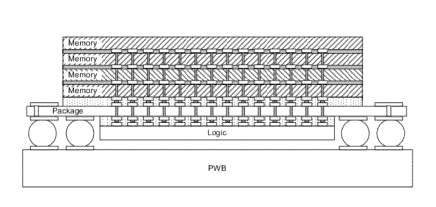
Rao R. Tummala and Venkatesh Sundaram from the School of Electrical and Computer Engineering at Georgia Tech have developed an ultra-small pitch structure that uses ultra-thin (20- to 200-mm) interposers containing ultra-high density through-via interconnections to achieve bandwidth rates of at least ~10 gigabytes/second (GB/s). Specifically, the 3D interposer connects two electronic devices that have the same (or similar) through-via density as the interposer. This innovative structure with its unprecedented density of interconnections—allowing 3D ICs to be stacked with or without TSVs—greatly increases bandwidth between the two devices.
The interposer can include pads that enable testing of the attached devices, and it can be constructed to provide thermal isolation or conduction, thereby easing thermal management. Devices can be connected vertically or in a side-by-side configuration to provide scalability.
- Scalable, with connections above, below, and beside the interposer
- Lower cost, less complex manufacturing through interposer-package integration
- Testable, both before and after device integration
- Thermally flexible, with options for localized thermal isolation and conduction
This technology is ideal for applications requiring a variety of heterogeneous ICs—such as logic, memory, graphics, power, wireless, and sensors—that cannot be integrated into a single IC.
This approach to three-dimensional (3D) packaging of integrated circuits (ICs) increases the logic-to-memory bandwidth of mobile devices without increasing power consumption. Two of the key factors influencing an IC’s bandwidth are the number of logic-memory interconnections (i.e., I/O density) and the length of those connections. Wire-bonded 3D packaging structures are limited in I/O density and interconnection length, preventing these structures from providing high bandwidth without a significant increase in power consumption. Other methods cannot be scaled to multiple chips due to signal delay. The newest scheme for achieving ultra-high bandwidth—called 3D ICs with TSVs (through-silicon vias)—is both expensive and complex in terms of chip manufacturing, power delivery, testability, reliability, and thermal management. There have been unsuccessful attempts to use less expensive ceramic or glass carriers with conductive through vias, but these cannot achieve the desired bandwidth. Therefore, an innovative approach was needed to achieve high bandwidth with a lower cost, better scalability, and less complexity.