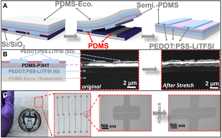
Georgia Tech inventors have created a versatile approach consisting of directly integrating stretchable components for a large-area transistor array through solution processing and a final single, mechanical peel-off step. As a result, the team has successfully fabricated semiconducting films with significantly improved mechanical elasticity and optical transparency, without affecting the film’s electronic conductivity. The semiconducting films are prepared by blending a small amount of either p-type or n-type commercial semiconductor polymers. The product is a self-organized versatile conjugated polymer film displaying an interpenetrating polymer network (IPN) formed in the semiconducting films, which is crucial for the observed enhancement of elasticity, optical transparency and charge-carrier mobility.
- Process is a readily implemented approach
- Films can be stretched by 100% with retention of their high charge carrier mobility
- Fabrication can be done with commercially available materials
- Newly fabricated high performance stretchable poly transistor arrays
- Enabling concept for currently non-available stretchable electronic technologies
- Production of stretchable optoelectronic devices on an industry scale
- Flexible and stretchable electronics for displays
- Stretchable wearable devices
- Devices suitable for epidermal applications, i.e., electronic skin
- Vast array of biomedical sensors
Stretchable microelectronics has garnered significant attention due to its use for wearable, epidermal and biomedical electronics. The current manufacturing process is constrained by its complexity and lack of scalability, and involves an elaborate synthesis process of intrinsically elastic semiconducting polymers and a multi-step transfer process. As a result, stretchable transistors are only applicable in small-area devices, and few studies have focused on the fabrication of large-area transistors. There is a need for a new approach involving scalable fabrication via a simple and robust, fully solution-processed methodology.

