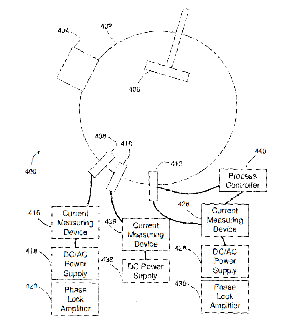
This new device and method enable users to measure the molecular flux leaving an effusion cell in a molecular beam epitaxy (MBE) system. Georgia Tech’s innovation consists of a metallic crucible with an optional dielectric shield. An optional metallic outer coating is designed to act as an insulator and guard terminal. The technology can be used in a closed-loop control system to provide in-situ flux control and stability by feeding an amplified current signal to a process controller. This configuration enhancement of an in-situ measurement (versus ex-situ) results in greater efficiency and enables a threefold improvement in speed compared with existing technology while eliminating unreliable variations and long-term drifts.
The device’s inner metallic container is connected to an electrometer or other current measurement device such as a lock-in amplifier. As the container is heated by external filaments, a small percentage of ions are emitted along with the neutral flux, which provides flux stability and control. Precision of up to 0.001% flux stability is possible when measurements are taken in an ideal setting. An optional AC or DC bias can be applied to the crucible to enhance the ion emission and to provide a phase-locked signal for further sensitivity and resolution.
- Efficient: Enables a 3x increase in MBE speed compared with metal organic chemical vapor deposition
- Controlled: Provides flux stability and control by enabling in-situ measurement of a signal related to the flux, achieving 0.001% flux stability under optimal conditions
- Reliable: Enables signal measurement in real time, providing high accuracy and reproducibility
- Economical: Solves many of the challenges of current-generation MBE machines (which increase device manufacturing costs), thereby providing a more affordable solution
Georgia Tech’s innovation enables replacement of effusion cells currently used in MBE systems, with potential benefits for:
- Solid state lighting
- Power semiconductors
- UV sterilization
- Compound transistors and optoelectronics devices
- Pseudomorphic high electron mobility transistors
- Photodetectors
- Light-emitting diodes (LEDs)
- Lasers
The technology is also useful for other thin-film deposition systems that employ evaporation or (with limitations) sputtering.
Thin-film deposition techniques require precise control of deposition parameters to produce complex structures needed for current and next-generation applications. Versatile MBE techniques address these needs by depositing single-crystal semiconducting, insulating, or metallic materials used in fabricating state-of-the-art electronic and opto-electronic devices. However, currently available MBE systems are not without limitations. Most are time-consuming, provide no real-time feedback, and are only marginally accurate when used for demanding structures—all challenges that increase device manufacturing costs. In addition, their flux measurements enable control only of the temperature of the source and not the flux itself, limiting stability. Georgia Tech’s innovation addresses these drawbacks with a highly precise device and method that enables faster deposition as well as greater stability and control than other MBE systems.

A schematic illustration of Georgia Tech’s system to measure in-situ molecular flux density.
