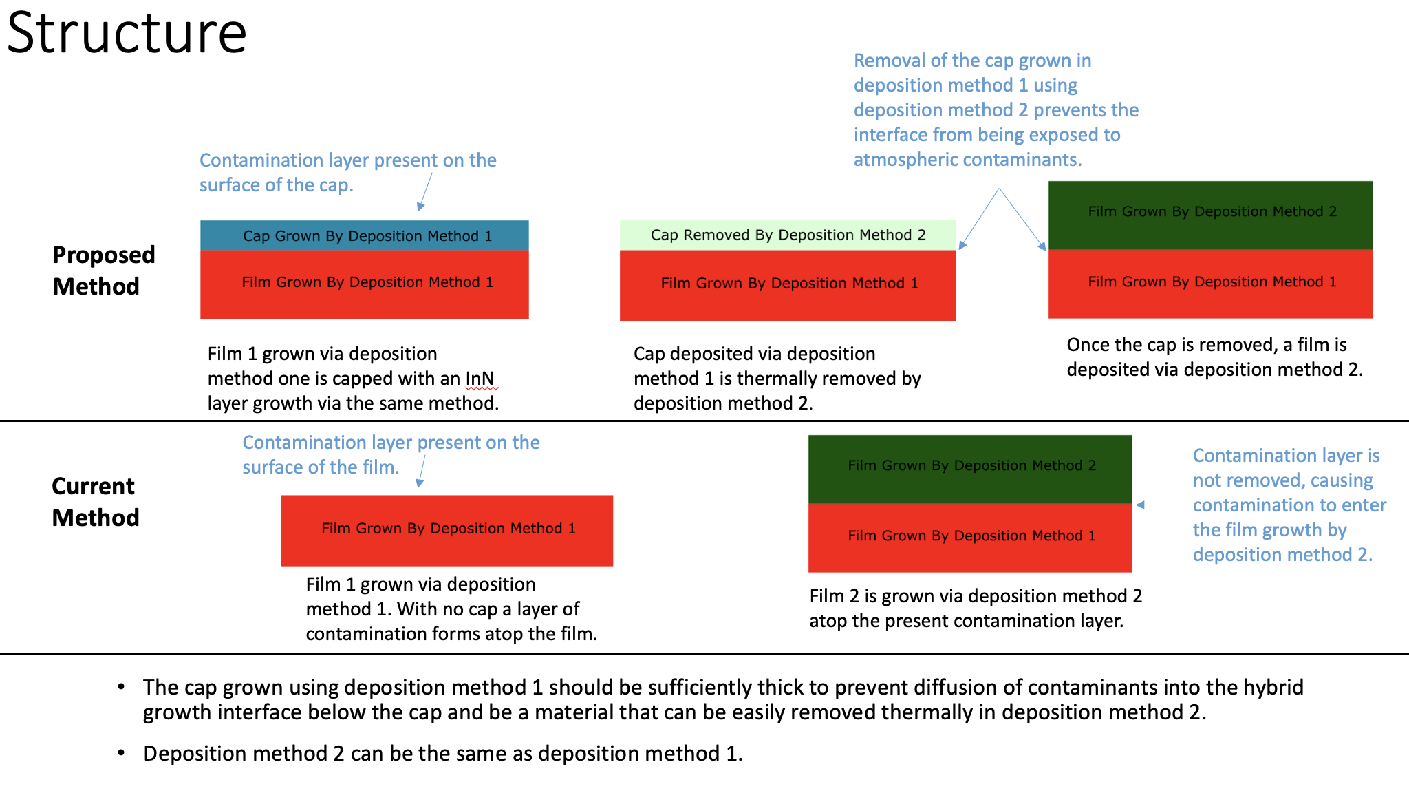
This method produces a protective layer or “cap” for semiconductor wafers, enabling the performance-improving promise of hybrid growth processes without the risk of contamination. Georgia Tech’s invention is designed to protect semiconductor wafers and improve their performance by eliminating the common problem of exposure to atmospheric contaminants, such as oxygen, carbon, silicon, and hydrogen. This exposure typically occurs in hybrid growth processes that use two separate systems to deposit the layers that compose the device. Without adequate protection, the wafer may be exposed to contaminants after the first layer is deposited. Georgia Tech’s method addresses this vulnerability by finishing the first deposition layer with an additional thin layer that can be easily removed during the second deposition without harming the underlying layer. This protective cap shields the device from contaminants during storage and/or transfer between deposition systems. During deposition of the second layer, the cap evaporates, removing any contaminants on its surface. The result is an ultra-clean, contaminant-free surface for the final layer, sidestepping the risk of defects and helping to improve device performance.
- Protective: Provides a thin protective layer or “cap” after the first layer is deposited, protecting the underlying structure from atmospheric contaminants
- Robust: Enables realization of the advantages of hybrid growth processes by eliminating performance-degrading contaminants and resulting defects
- Advanced: Offers superior protection against contamination compared with simple chemical cleaning methods utilized in other systems, especially against impurity species such as oxides
- Enabling: Addresses a critical shortcoming of other technologies that currently offer no way to efficiently transfer samples between deposition chambers without exposing critical interfaces to contamination
- Flexible: Works for processes that utilize two deposition chambers—be they the same or different types (e.g., MOCVD and/or MBE)
This technology provides contamination protection during hybrid growth processes for production of semiconductor wafers, enabling better performance for devices such as:
- LEDs
- Lasers
- Transistors
- Solar cells
Hybrid growth approaches to producing III-nitride-based semiconductor wafers have been shown to improve performance. This is due to the fact that no one deposition system can provide the best of all needed benefits. For instance, metal organic chemical vapor deposition (MOCVD) results in growth of high-quality LED and solar cells structures, but molecular-beam epitaxy (MBE) deposition is better suited to doping. To get the benefits of both, a process that leverages both types of deposition systems is advantageous but exposes samples to contamination when transferring between systems. These impurities get incorporated into any film or layers grown on top of them, resulting in defects and degrading performance. Georgia Tech’s method of producing a protective layer that can be evaporated during the deposition of the second layer directly addresses this problem.

Georgia Tech’s method provides distinct protection and performance advantages compared with current methods that offer no cap to shield the structure from contamination.
