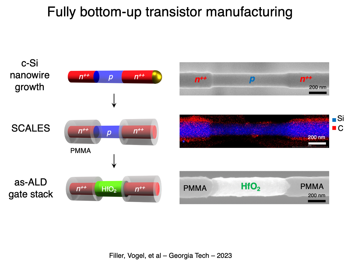
Georgia Tech inventors have developed a fabrication method competent for large production scale that is entirely “bottom-up” for MOSFETs. This approach builds the layers of nanowires from the bottom up, as opposed to removing material from a bulk sample, as in the top-down fabrication method. This fabrication method utilizes the single crystallinity of semiconductor nanowires to provide high electron carrier motilities and bottom-up nanowire growth to achieve the chemical structure needed for the nanowires. This approach allows for large-scale fabrication and patterning of high-performance nanowires. When utilized in MOSFETs the nanowires allow for exceptional device switching speeds at low voltages.
- Scalable – Eliminating the cost and time associated with top-down patterning enables large-scale manufacturing
- High Performance – Achieves switching speeds well beyond 1 GHz at supply voltages near 0.5 V
- Adaptable – Device dimensions can be readily scaled as transistor fabrication techniques advance
- Artificial skins
- Smart structures
- Smart dust – A simple computer light enough to be suspended in air formed from electronic systems
- Electronic medicines
Applications ranging from artificial skins to smart structures are demanding a fundamentally new electronics manufacturing system due to a long-standing trade-off between the performance and manufacturing scale of electronics. Production of active devices; circuit components capable of controlling current such as metal oxide semiconductor field effect transistors (MOSFETs), either exhibit high performance or large production scale, but not both. A manufacturing system, enabling large production or high-performance MOSFETs, is crucial to the development of electronic applications.

Schematic illustration of and representative data from each step in the transistor fabrication process, including single-crystal Si nanowire growth, selective polymer masking, and area-selective atomic layer deposition (ALD).
