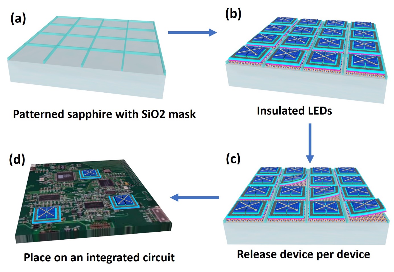
Georgia Tech innovators have developed a technique for large-scale growth and fabrication of III-Nitride (III-N) devices integrated with other technologies to form a high-performance heterogenous system with increased functionality. A key component of the innovation is a mechanical liftoff technique that enables hybrid integration and dicing-free pick-and-place applications.
The technique uses 2D hexagonal boron nitride (h-BN) as a mechanical release layer and patterned sapphire with a silicon oxide (SiO2) mask to achieve localized van der Waals epitaxy of high-quality gallium-nitride (GaN)-based structures. After process fabrication, devices from micron to millimeter size can be individually placed on a foreign substrate without the need for a dicing step. This approach further reduces h-BN delamination on large-diameter substrates, as each h-BN region is smaller and has independent device structures.
The innovation is scalable for any wafer size, can be applied to other types of nitride-based devices, and is compatible with commercial pick-and-place handlers for mass production. This advance will allow III-N devices to be used more flexibly in a broader range of applications, including flexible electronics.
- High performance: Enables simple and fast transfer to foreign substrates with an automated pick-and-place technique
- Compatible: Can be used to transfer devices of any shape and size—from micron to millimeter
- Efficient: Allows reuse of the growth wafer, lowering production costs
- Safe: Eliminates the need for time-consuming and potentially hazardous chemical treatments
- Adaptable: Can be conducted in any metal organic chemical vapor deposition (MOCVD) growth chamber size
- Hybrid integrated electronics
- Flexible/Wearable opto-electronics
- High-power electronic devices
- Ultraviolet (UV) light sources, sensors, and detectors
- µ-LEDs to cm2-LEDs
- High-concentration PVs
As the electronics industry enters an era of acceleration and disruption, heterogeneous integration will become an important component for emerging technology fields, such the Internet of Things (IoT) and advanced communication technology. One approach to heterogenous integration is the transfer of epilayers from their native growth substrate to a dissimilar receiving substrate. A range of epitaxial layer separation approaches have been developed, such as laser liftoff and chemical liftoff, but their use is limited by high costs and long processing times.
This Georgia Tech innovation utilizes a mechanical liftoff technique that is fast and results in smooth separated surfaces, facilitating epitaxial growth on large wafers and enabling the development of industrial-scale III-Nitride-based integrated devices.

Epitaxy and fabrication of GaN-based light-emitting diodes (LEDs) on 2D h-BN using dielectric patterns on sapphire substrates. (a) A large-surface sapphire wafer patterned into small areas onto a SiO2 grid. (b) Insulated grown and fabricated devices on h-BN. (c) Devices released one by one from the sapphire wafer. (d) Devices placed on an integrated circuit.

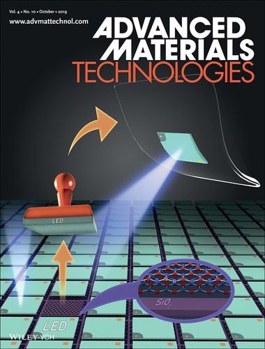
The innovation is featured on the cover of the October 2019 issue of the journal Advanced Materials Technologies.
