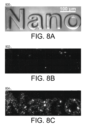
Zhong Lin Wang and Caofen Pan from the School of Materials Science and Engineering at Georgia Tech have used piezotronic and piezophototronic effects to develop pressure sensor arrays that have demonstrated an unprecedented level of spatial resolution. Specifically, their piezotronic pressure sensor array achieved a spatial resolution of 120 μm, while their piezophototronic pressure sensor array high the ultra-high mark of 2.7 μm. The technology provides stable, fast response, and parallel-reading detection of spatial pressure distribution.
This ground-breaking pressure sensor technology consists of an array of elongated light-emitting piezoelectric nanostructures containing n-type semiconductor material (e.g., zinc oxide [ZnO] nanowires) connected to a p-type semiconductor layer (e.g., gallium nitride [GaN]), creating p-n junctions. Each piezoelectric is surrounded by an insulative resilient medium layer (e.g., poly[methyl methacrylate] or PMMA) and electrically coupled to a transparent planar electrode. Applying a biasing voltage causes each nanostructure to emit light at an intensity that indicates the level of compressive strain.
- Extremely sensitive: This sensor array provides 1,000x higher sensitivity than other technologies.
- Improved performance: The technology is fast-responding and stable.
This technology would benefit applications that require highly accurate/sensitive pressure sensing:
- Robotics
- Computer hardware
- Mobile devices
- Security systems
- Medicine
- Manufacturing
This technology takes a dramatic step forward in the development of high-resolution pressure sensors. The ability of electronics to mimic human senses—particularly our sense of touch—has long been a significant challenge for robotics and other computer applications. Touch pads are used frequently in today’s electronics, but their resolution is nowhere near that of nerve endings in skin. Truly replicating the sense of touch requires massive pressure sensor arrays that are highly sensitive and fast while offering high spatial resolution. Current efforts to develop such arrays use assembled nanowires, organic transistors, or microstructured rubber layers that sense changes in capacitance or resistance. Although these arrays achieve millimeter-scale resolution, human skin has a resolution of better than 50 mm.

