Current permittivity measurement techniques either lack precision or are costly
In industries such as aerospace and semiconductors, precise characterization of material permittivity is critical. Material scientists and engineers regularly seek out methods of characterizing the properties of novel materials, including electrical properties, to satisfy various design criteria or as inputs to simulation models. Current permittivity characterization measurement practices either use broadband transmission line techniques (e.g., focused beam, coaxial airline, waveguide measurements), or they use narrowband resonant techniques (e.g., resonant cavities, open-boundary Fabry-Perot resonators, split-cylinder resonators). Broadband methods lack the precision needed in classifying the permittivity of materials tested. Current narrowband resonant methods achieve the sensitivity but only at single or narrow ranges of frequencies. To obtain broadband data, multiple individual measurements must be taken, which increases time and expense considerably.
Metasurface measurement method for complex permittivity reduces time and cost
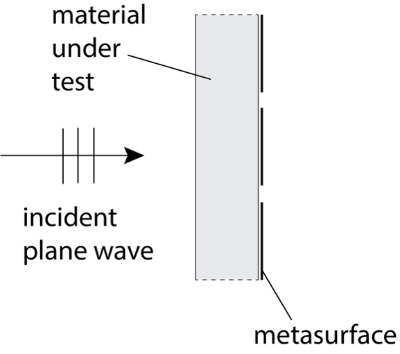
This hybrid resonance/transmission method attaches a highly resonant periodic array to a dielectric sample and takes measurements using a broadband-focused beam system. Placing a thin, conductive, two-dimensional screen with a periodic pattern, or metasurface, against a planar dielectric sample creates a transmission or reflection response that is sensitive to the loss tangent of the sample. The geometry of the metallic pattern on the metasurface determines the center frequency and bandwidth of the resonance. Scattering parameters are measured as this focused beam system illuminates the sandwiched structure to approximate plane-wave-like incidence. The magnitude of response at the resonant frequency depends linearly on the loss tangent of the sample material.
This method characterizes the complex permittivity of a dielectric material at radio frequencies, including microwave and millimeter wave, quickly and at lower cost than with existing techniques.
This technology also supports the integration of active electronic circuitry. This enables digital or analog control of circuitry, resulting in changes to the metasurface properties and allowing measurements of disparate frequencies with a single active metasurface.
- Low cost: The metasurface is comparatively inexpensive, reducing cost via labor savings and lower material costs.
- Faster: Compared to current techniques, measuring multiple metasurfaces takes substantially less time and labor to acquire data.
- Configurable: The electronically reconfigurable system allows integration of active electronics for tunability and eliminates the need for several masks to achieve the needed bandwidth.
- Nondestructive: The technique allows repeated use of a single planar dielectric sample with multiple metasurfaces and for multiple measurements.
- Versatile: Unlike existing techniques that require precisely dimensioned samples of different sizes for each frequency, the technology can measure individual frequencies by swapping out only the metasurfaces, which can be used on a wide range of sample thicknesses.
- Aerospace
- Electromagnetic properties of materials used for communication, navigation, and radar purposes, which must be known and closely integrated with radio frequency and infrared technologies
- Semiconductors
- In-situ characterization of various dielectric films that are critical to final device performance, such as the SiO2 layer in silicon processing
- State-of-the-art semiconductor packaging where dielectric consistency of the chip interconnects enables operation at effective microwave frequencies

Placing the metasurface against a planar dielectric material sample creates a transmission or reflection response that is sensitive to the loss tangent of the material under test.
