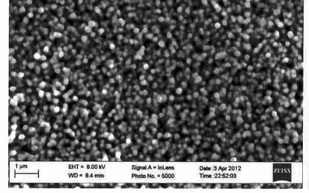
Zhong Lin Wang, and Ken Pradel from the School of Materials Science and Engineering at Georgia Tech have developed a fabrication technique to synthesize arrays of long aligned antimony (Sb) doped p-type ZnO nanowires in a low temperature, aqueous environment. Specifically, a ZnO precursor, such as zinc nitrate (Zn(NO3)2) is mixed with hexamethylenetriamine and PEI. These components are then mixed thoroughly with water to evenly distribute the constituents and ease processability. Next, a dopant solution containing antimony acetate (SbAc3), glycolic acid, and sodium hydroxide is added to the Zn precursor in the desired concentration. This solution is preheated for 1 hour prior to adding it to the substrate. The substrate consists of glass slides sputter-coated with a 150 nm layer of ZnO separated by a thin layer of indium tin oxide (ITO) in order to improve adhesion. After 24 hours the substrate was removed and rinsed. The substrate was dried by placing it in an oven for 1 hour, which removed any organic residue. The doped nanowires were characterized for morphology, composition, and electrical properties.
- Can be used to create p- and n-type homojuntion ZnO nanowires.
- Nanowires as long as 340 µm were fabricated in a reproducible manner.
- Fabrication technique employs low temperature conditions in an aqueous environment.
- Gentle process amenable to flexible electronics and various substrates.
- Various dopant concentrations can be employed depending on the desired properties of the resulting nanowires.
This novel manufacturing technique addresses the needs of flexible electronics through a low-temperature and aqeous process that expands the potential substrates that can be used. Potential commercial uses include ZnO-based optoelectronic devices applications, such as light emitting diodes and photovoltaics, as well as photosensing applications in both commercial and military applications.
Nanostructured zinc oxide (ZnO) materials have been the subject of intense research due to their unique electronic, optic, and photonic properties. ZnO is naturally an n-type semiconductor, but of late, there is growing interest in the fabrication of p-n homojunction nanowires where a single ZnO nanowire has both p and n-type regions. A material such as this would find utility in single wire LEDs and logic circuits. However, harsh synthesis methods limit the substrates on which this material can be grown. A gentle approach is needed in order to apply this promising material to flexible electronics.

