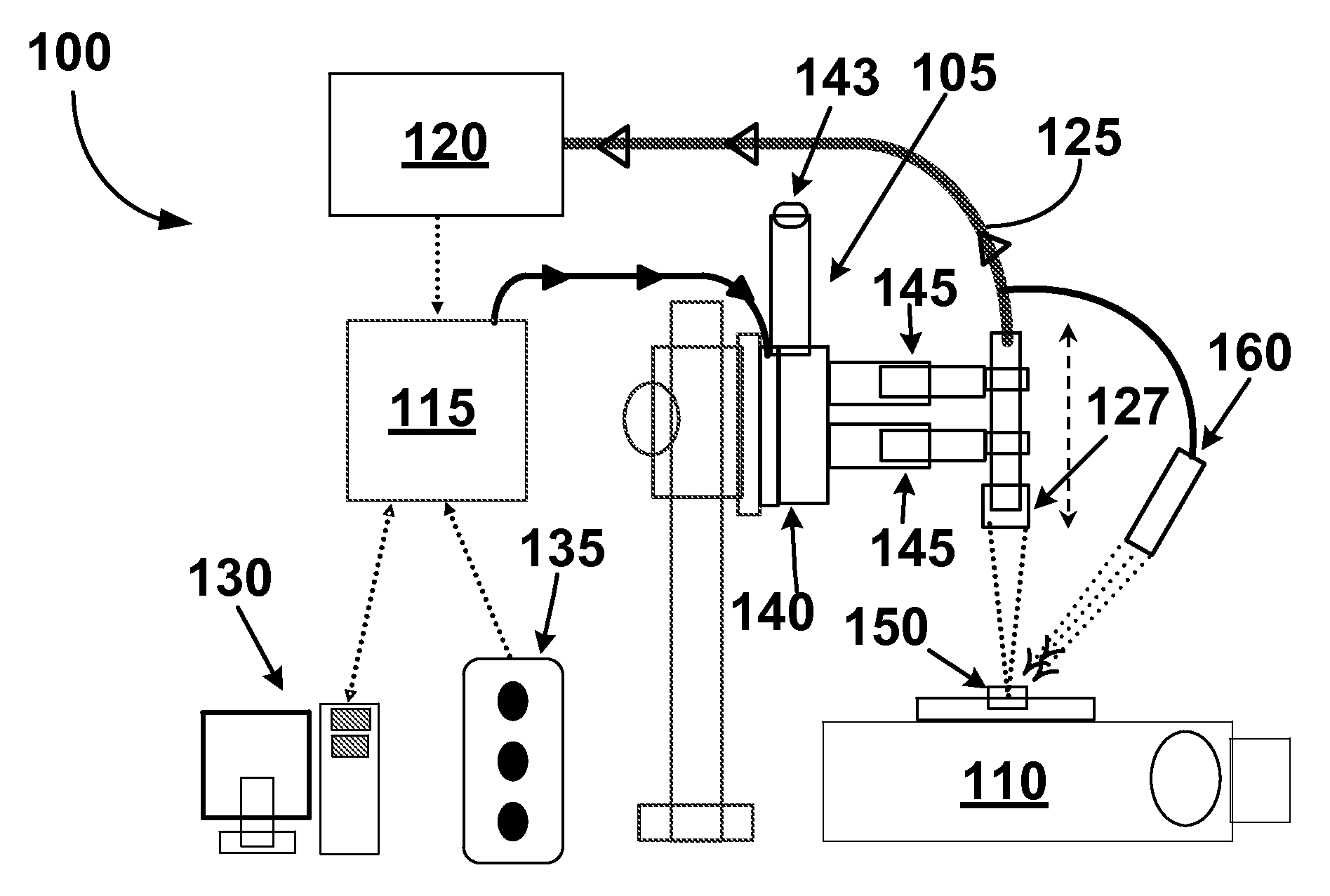
Georgia Tech researchers have developed a high-speed autofocus system and method. This system includes a laser module, an interferometer module, and a system controller. The laser can produce laser pulses to excite a device such as a silicon wafer, chip capacitor or chip packaged/silicon die containing a plurality of solder bumps into vibration. The interferometer module can be disposed to receive reflected laser energy from the device to sense vibration displacements created in the device with the laser pulses. This invention also include noncontact, nondestructive inspection techniques for investigating solder bump and joint integrity. This system can also detect misaligned, bridged, shorted, missing, cracked, voided, delaminated, non-wetted, partially connected, open, excessive, head-in pillow, non-wetted, and starved solder bumps.
- High-speed
- Fully noncontact
- Nondestructive inspection techniques for investigating solder bump and joint integrity
- Easily detect misaligned, bridged, shorted, missing, cracked, voided, delaminated, non-wetted, and starved solder bumps
- Printed circuit board assembly (PCBA) manufacture
- Systems and methods to test integrity of solder joints or bumps used to attach integrated circuit chips, chip packages, and chip capacitors to PCBs and substrates
Integrated circuit (IC) packages provide power and signal interconnects while also providing protection and heat dissipation to IC electronics. For most applications, conventional ICs use lead-frame package designs like a small-outline integrated circuit for power and signal distribution to the printed circuit board (PCB) or substrate. These packages have made surface-mount devices popular. They have, however, had difficulty being integrated into performance applications where a high density of interconnects is needed and where size and weight are important factors.

