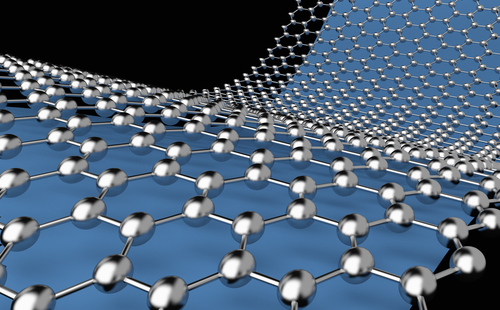
Inventors at Georgia Tech have developed a method of applying a gate to graphene that does not require the use of a dielectric layer. Graphene is deposited on a non-conductive substrate such as silicon oxide or silicon carbide. A metal gate, composed of a metal with a high contact resistance with graphene, is placed on a portion of the graphene structure. Next, two electrical contacts are placed on either side of the graphene structure so that the metal gate is between the two contacts. The two metal contacts function as a source and a drain while the metal layer functions as a gate. In spite of the direct physical contact between the metal and the graphene, the contact resistance between the two is large enough that a significant potential difference can be maintained without causing undesirable large currents to flow between them.
- Does not require the application of a dielectric layer to the graphene
- Graphene does not need to be chemically modified
- Maintains quality of graphene
- Only small potential differences need to be applied to the gate in order to produce large conductivity changes in the graphene layer
- Development and improvement of graphene components suitable for electronic and photonic applications
- Field effect transistors
The conductivity of graphene depends on the density of charge carriers (electrons or holes) in the material. The magnitude of a current supplied by an applied voltage can be modified through the use of an electrostatic gate. Existing electronic devices that utilize graphene employ a gate composed of a dielectric material deposited on the graphene and a metal layer deposited on the dielectric material. The effectiveness of the gate is determined by the potential difference necessary to produce the desired conductivity change in the graphene. However, it is difficult to apply a dielectric material to graphene, and the graphene must be chemically modified to promote dielectric adherence. This modification often leads to degradation in the quality of the graphene. Furthermore, large potential differences need to be applied between the gate and the graphene in order to produce a suitable gating effect because of difficulty in applying sufficiently thin dielectric layers to graphene.

