Current D-band millimeter wave VMPSs have limitations
While high-performance wideband millimeter wave (mmWave) transceivers at D-band (110–170 GHz) offer greater available bandwidth for high data rate communications, there is greater path loss due to atmospheric attenuation. To address this, phased arrays can be utilized to achieve acceptable, effective isotropic radiated power and beam steering over long distances.
Existing mmWave VMPSs at or near D-band each have challenges, such as achieving:
- High gain but suffering from high power consumption and narrow bandwidth
- Wide bandwidth and very low power consumption but having high insertion loss
- Moderate gain, moderate bandwidth, and low power consumption but having difficulties achieving simultaneous wide bandwidth and low loss
Innovative D-band VMPS achieves very wide bandwidth and moderate gain with low power consumption
This D-band VMPS achieves greater than 30 GHz bandwidth at a center frequency of 127.5 GHz—the widest of any mmWave VMPS implemented in silicon. Using a novel, transmission line–based delay line topology, this 4-bit D-band silicon-germanium (SiGe) VMPS generates differential quadrature signals that are weighted by four identical variable gain amplifiers (VGAs) and cascaded with a buffer amplifier at the output to compensate for losses. This results in very wide bandwidth, moderate gain, and low power consumption, which combined enable higher speed communications.
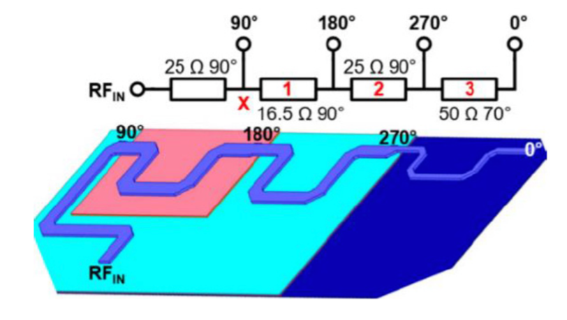
- Faster communications: Rather than using standard lumped, distributed element couplers, and baluns, this technology uses tapered delay lines at the input to generate differential quadrature signals that enable wider bandwidth and result in higher speed communications.
- Moderate gain: This VMPS reaches a moderate gain of 1.5 decibels (dB), while simultaneously achieving higher 3-dB bandwidth (35 GHz) at a center frequency of 127.5 GHz and significantly higher fractional bandwidth (27.5%) than any other mmWave VMPS in silicon.
- Low power consumption: The VMPS has an average power consumption of 20.3 mW across all states with voltage at the common collector of 1.5 V supplying an average current of 13.5 mA to the VGAs and buffer amplifier.
Designed for use in communications applications such as:
- 6G cellular communications (>100 GHz)
- Next-generation wireless communications
- Internet of Things

Schematic and 3D layout of the differential quadrature delay lines. Tapering and changing the ground plane may be used to achieve the wide range of impedances of the delay lines.

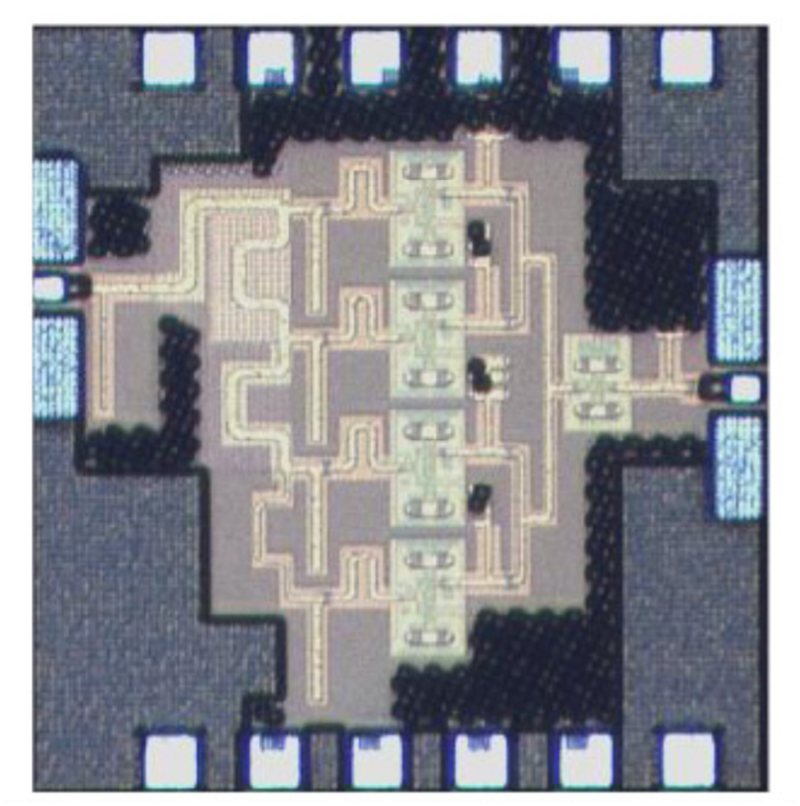
The die micrograph of fabricated VMPS with total die area of 1.21 mm2 and core area of 0.81mm2
